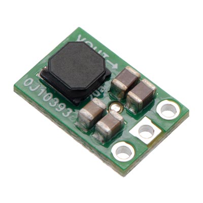
2.5-9V Step-Up/Step-Down Voltage Regulator
- үнэ: 43,000 төг
2.5-9V Fine-Adjust Step-Up/Step-Down Voltage Regulator S9V11MA
Pololu item #: 2869
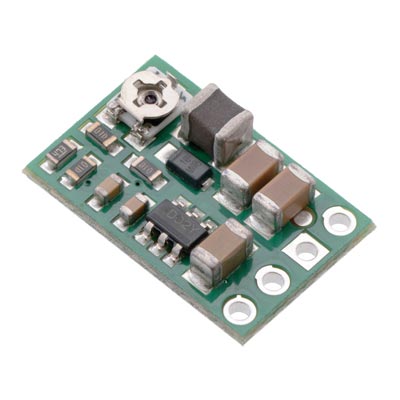
The S9V11MA switching step-up/step-down regulator efficiently produces a finely adjustable output between 2.5 V and 9 V whether it is higher or lower than the input voltage, which can range from 2 V to 16 V. (Note: minimum start-up voltage is 3 V, but it operates to 2 V after that.) The compact (0.5″ × 0.6″) module can supply a typical output current of up to 1.5 A when the input voltage is close to the output voltage.
Dimensions
| Size: | 12.7 × 15.3 × 6.4 mm |
|---|---|
| Weight: | 0.8 g |
General specifications
| Minimum operating voltage: | 2 V |
|---|---|
| Maximum operating voltage: | 16 V |
| Maximum output current: | 1.5 A |
| Minimum output voltage: | 2.5 V |
| Maximum output voltage: | 9 V |
| Reverse voltage protection?: | N |
| Maximum quiescent current: | 1 mA |
Identifying markings
| PCB dev codes: | reg20b |
|---|---|
| Other PCB markings: | 0J10534 |
Details for item #2869
Features
- – Input voltage: 2 V to 16 V (note: this regulator requires 3 V to start, but it can operate down to 2 V after startup)
- – Output voltage: 2.5 V to 9 V (precision-adjustable using built-in 12-turn potentiometer)
- – Typical maximum continuous output current: 1.5 A (when input voltage is close to the output; the Typical efficiency and output current section below shows how the achievable continuous output current depends on the input and output voltages)
- – Power-good indicator can be used to tell when the regulator has reached and is maintaining its target output voltage
- – Power-saving feature maintains high efficiency at low currents (quiescent current is less than 1 mA while enabled and approximately 7 µA per volt on VIN when regulator is disabled)
- – Integrated over-temperature and short-circuit protection
- – Small size: 0.5″ × 0.6″ × 0.25″ (12.7 × 15.3 × 6.4 mm)
Using the Regulator
During normal operation, this product can get hot enough to burn you. Take care when handling this product or other components connected to it.
Connections
The step-up/step-down regulator has five main connections all located along the same edge of the board: the output voltage (OUT), ground (GND), the input voltage (IN), an enable input (EN), and a power good indicator (PG). The board also contains a through-hole labeled SEL that is not used on this version of the regulator.
The input voltage, VIN, should be between 3 V and 16 V when the regulator is first powered. After it is running, it can continue operating down to 2 V. Lower inputs can shut down the voltage regulator; higher inputs can destroy the regulator, so you should ensure that noise on your input is not excessive, and you should be wary of destructive LC spikes (see below for more information).The output voltage, VOUT, is determined by the trimmer potentiometer position. See the Setting the output voltage section below for details.
The regulator, which is enabled by default, can be put into a low-power sleep state by reducing the voltage on the EN below 0.7 V, and it can be brought out of this state again by increasing the voltage on EN past 0.8 V. The quiescent current draw in this sleep mode is dominated by the current in the 100 kΩ pull-up resistor from ENABLE to VIN, which is approximately 7 µA per volt on VIN (e.g. approximately 20 µA with 3 V in). The tight tolerance of the enable input allows a precise low-VIN cutoff to be set, such as with the output of an external voltage divider powered by VIN, which is useful for battery powered applications where draining the battery below a particular voltage threshold could permanently damage it.
The “power good” indicator, PG, is an open-drain output that goes low when the regulator’s output falls below around 90% of the nominal voltage, including when the enable pin is held low. The power good indicator is held low until the output reaches 95% of the nominal voltage when it is powering up or coming out of low-power mode. Otherwise, the PG pin is high-impedance, so an external pull-up resistor is required to use this pin.
Included hardware
Setting the output voltageThe through-holes are arranged with a 0.1″ spacing along the edge of the board for compatibility with standard solderless breadboards and perfboards and connectors that use a 0.1″ grid. You can solder wires directly to the board or solder in pieces of the included breakaway 6 ×1 straight male header strip or the 5×1 right-angle male header strip as desired.
 |
The output voltage of the regulator is controlled with a 12-turn precision potentiometer. Turning the potentiometer clockwise increases the output voltage, and it can be measured using a multimeter.
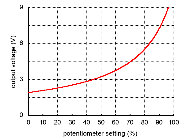 |
| Output voltage settings for the 2.5-9V Fine-Adjust Step-Up/Step-Down Voltage Regulator S9V11MACMA and S9V11MA. |
|---|
Please note that the output voltage can be set below 2.5 V at the low end of the potentiometer’s range and above 9 V at the high end. While this is not likely to damage the regulator, it might not work reliably or its output could become unstable when the output voltage is not within the recommended 2.5 V to 9 V range.
The output voltage can be up to 3% higher than normal when there is little or no load on the regulator. The output voltage can also drop depending on the current draw, especially when the regulator is boosting a lower voltage to a higher one (stepping up), although it should remain within 5% of the set voltage.
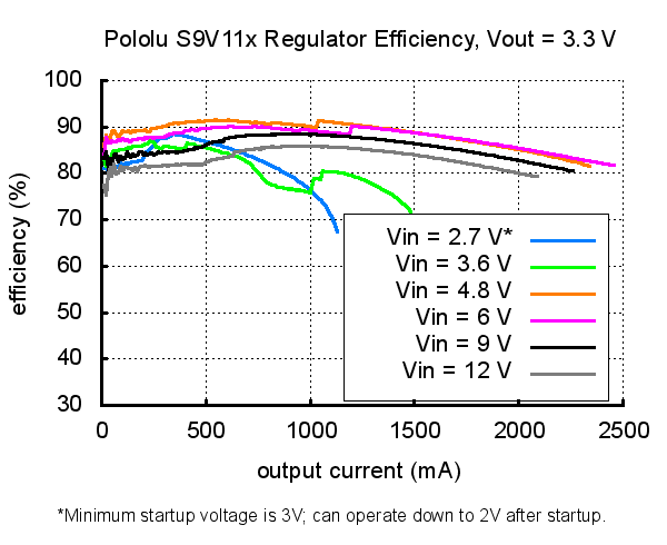
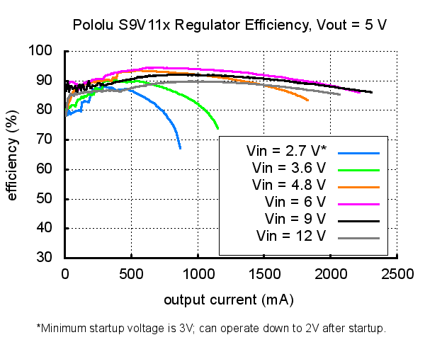
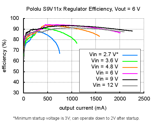
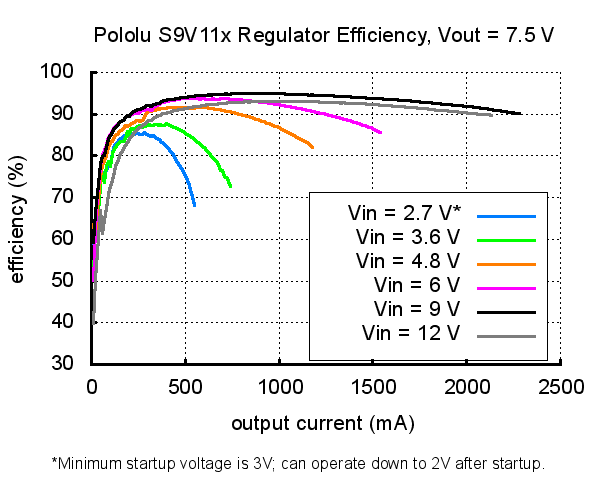
Typical efficiency and output current
The efficiency of a voltage regulator, defined as (Power out)/(Power in), is an important measure of its performance, especially when battery life or heat are concerns. As shown in the graphs below, this family of switching regulators typically has an efficiency of 85% to 95%. A power-saving feature maintains these high efficiencies even when the regulator current is very low.
 |
 |
 |
 |
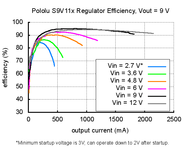 |
The maximum achievable output current of these regulators varies with the input voltage but also depends on other factors, including the ambient temperature, air flow, and heat sinking. The graph below shows maximum output currents that these regulators can deliver continuously at room temperature in still air and without additional heat sinking. Depending on the input and output voltage, these regulators can temporarily deliver over 2 A, though they will typically quickly overheat under such conditions and go into thermal shutdown.
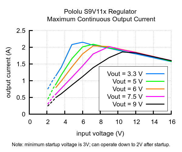 |
Note that the startup current for input voltages above the regulated output voltage is limited to approximately 700 mA, and currents in excess of this are only available after the output has finished stabilizing. For input voltages below the output voltage, the available start up current decreases linearly with the input voltage to approximately 0.3 A with an input of 3 V. Large capacitive loads will generally not pose a problem because they will gradually charge up even with the current limit active, so while they may increase the time it takes an S9V11x family regulator to start up, the regulator should still eventually stabilize. A purely resistive load, however, could prevent the regulator from ever reaching the desired output voltage. For example, if the output of the regulator is 5V and you put a 5 Ω resistor between VOUT and GND and then apply power to the regulator, the output voltage will never rise past 3.5 V, the voltage at which the current draw reaches the 700 mA limit. As such, this family of regulators is intended for applications like robotics, where any large loads are controllable and can be applied only after the regulator has finished starting up.
LC Voltage Spikes
When connecting voltage to electronic circuits, the initial rush of current can cause voltage spikes that are much higher than the input voltage. If these spikes exceed a regulator’s maximum voltage, the regulator can be destroyed. If you are connecting more than about 9 V, using power leads more than a few inches long, or using a power supply with high inductance, we recommend soldering a 33 μF or larger electrolytic capacitor close to the regulator between VIN and GND. The capacitor should be rated for at least 20 V.
More information about LC spikes can be found in our application note, Understanding Destructive LC Voltage Spikes.